
What are the manufacturing processes for flexible PCB boards?
manufacturing processes for flexible PCB boards
The manufacturing process for flexible PCB boards involves a few distinct steps. They are different from standard PCBs because they must support bending and expansion over long periods of time without breaking. This is why they are not as easy to produce as standard PCBs, but they can still be made with good results. The first step is to design the board using a computer-aided design (CAD) program. This will include the layout of the circuit and the placement of components. It will also specify any requirements for the flexibility or bending of the circuit.
The next step is to select a substrate material. There are several choices, including polyimide and polyester film. These materials are often used in flexible pcb board because they offer excellent electrical insulation properties, high-temperature resistance, and pliability. A conductive material is then placed on the substrate to create the electrical pathways for the circuit. The most common conductive material for flexible PCBs is copper because it offers a good balance of conductivity, flexibility, and durability.
After the conductive material is laid on the substrate, it must be etched to create the circuit pattern. The etching process can be performed by dipping the laminate in an etch bath or spraying it with an etchant solution. Both sides of the laminate are etched to achieve the desired circuit pattern. The etching process is followed by a copper plating process to establish the electrical connections between the layers of the rigid-flex.
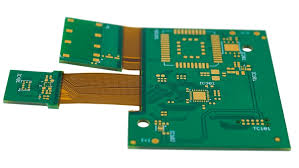
What are the manufacturing processes for flexible PCB boards?
Next, the layer structure is bonded together with an adhesive. This adhesive can be a thermosetting epoxy or an acrylic-based system. This step is crucial for the structural stability of a flex circuit. After the layer structure is bonded, it can be cut and trimmed to ensure that the final product meets the precise size and shape required for its end-use application.
Once the flex circuit is trimmed and cut, it must undergo surface treatment. This is done to protect the copper from environmental contaminants. This surface treatment can also make the finished product EMI-resistant, waterproof, and flame retardant.
The final fabrication step is lamination. The final product consists of two, 2-layer flex circuits embedded between three rigid sections. It is important to note that the flex-rigid PCB must be designed with this process in mind because it requires special lamination techniques and a rigid-flex layer stack-up. The flex-rigid PCB must have plated through holes for each flex section, as well as the corresponding plated through holes on the rigid sections.
Lastly, the PCB must undergo the electrical testing and power-on self-test process to verify its functionality. Then, it can be packaged and shipped for use. It is important to test the flex circuit before it is used in production because the testing can identify any defects or errors that might affect its performance. In addition, it can also help determine the best way to improve the flex circuit’s design. This will help reduce the cost of production and maximize its usefulness.