
Understanding the Intricacies of an RF Board
Intricacies of an RF Board
An rf board is a printed circuit board that is specifically designed to support radio frequency communication standards like Bluetooth, RFID, ZigBee, cellular and LoRa. These boards use precise 50- or 75-ohm impedance-matched transmission lines to minimize reflections, resulting in high-quality audio and data signal transfers with the ability to handle large amounts of electrical power over long distances without attenuation or degradation. They also feature grounding structures and guard traces to minimize interference between adjacent circuits.
PCBs have been the backbone of modern electronic devices for decades, enabling them to function in a myriad of applications, from home and office electronics to advanced industrial and military equipment. However, RF circuits differ significantly from traditional PCBs in their specialized design and materials. RF PCBs require a high-frequency dielectric constant with a low loss tangent and excellent thermal properties to handle the elevated temperatures of their operation. Additionally, they need to be able to tolerate high levels of radiation and EMI noise as well as operate within a tight impedance tolerance.
Understanding the intricacies of rf board is vital for creating a design that will meet and exceed the required performance requirements. To begin, it is crucial to determine the application’s operating frequency range, signal bandwidth, power level, noise specifications and dimensions of the RF components and their connection points on the board. Once these requirements have been established, the RF designer can create a high-level system circuit diagram and develop the corresponding CAD schematics for each layer in the PCB’s multilayer design.
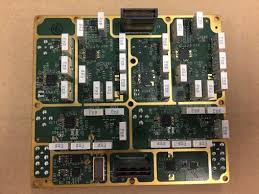
Understanding the Intricacies of an RF Board
The next step is to choose the appropriate PCB laminate and bondply material to ensure that the RF circuit will be able to achieve its desired performance characteristics. For optimum results, the laminate used in an RF PCB should offer good dielectric constant (DK), low loss tangent and excellent thermal properties that are consistent over a wide range of frequencies, as well as be stable against environmental vagaries. Using a hybrid laminate stackup is often necessary to achieve these requirements, with the top layer of the stackup dedicated to supporting RF transmission lines and circuits, while the inner layers are used for digital signals, routing and power.
Once the RF layer has been chosen, the remaining layers should be devoted to providing a solid ground plane, shielding against electromagnetic interference and the creation of ground loops. In addition, the RF layer traces should be arranged in a way that maximizes the signal’s length while keeping its characteristic impedance as close to 0 ohms as possible.
Finally, the RF designer must ensure that proper signal isolation is achieved by separating the RF signals from those of other devices on the PCB through the use of bypass capacitors and decoupling circuits. It is also recommended to place the RF traces far from any high-speed digital traces and power supply lines, as coupling between these different paths can lead to significant attenuation and distortion of the RF signal.