
How do you optimize a Pcb production for manufacturing?
optimize a Pcb production for manufacturing
Optimizing PCB production for manufacturing is crucial for ensuring that the final product meets design specifications, is produced efficiently, and is cost-effective. In the competitive landscape of electronics manufacturing, optimizing the PCB production process is key to maintaining quality while reducing production time and cost. This process involves several key considerations, from design to material selection and assembly. Below are some strategies to optimize PCB production for manufacturing.
One of the most important steps in optimizing pcb production is to start with a well-thought-out, manufacturable design. The complexity of the PCB design can have a direct impact on the ease and cost of manufacturing. Designs with fewer layers, simpler traces, and fewer components are generally easier to produce and less expensive. Avoiding intricate routing or overly small pads can help prevent issues during the production phase, ensuring that the PCB can be fabricated quickly and with fewer chances of errors.
Furthermore, designers should consider the design rules of the manufacturing process, such as minimum trace width, spacing between traces, and via sizes. By designing within these constraints, manufacturers can streamline the production process and reduce the risk of rework or failure.
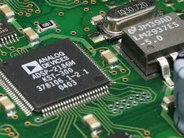
How do you optimize a Pcb production for manufacturing?
Choosing the right materials for the PCB is a critical factor in optimizing production. The material affects the electrical performance, thermal stability, and durability of the PCB. While traditional FR4 (fiber-reinforced epoxy laminate) is commonly used in many applications, specialized materials may be required for high-frequency or high-performance designs. For instance, materials with low dielectric constants are ideal for high-speed circuits to reduce signal loss.
When optimizing for manufacturing, selecting readily available materials that align with the design requirements can help minimize costs and lead times. Standardized materials that the manufacturer is familiar with will also result in more efficient production processes, reducing the risk of defects and delays.
Efficient component placement plays a significant role in optimizing PCB production for manufacturing. The goal is to minimize the amount of time and resources needed to assemble the PCB while ensuring that the components are placed correctly for functionality. Grouping components with similar functions together, such as placing passive components near their respective ICs, reduces routing complexity and simplifies the assembly process.
Additionally, it is important to ensure that components are placed in a way that facilitates efficient soldering, especially when considering automated assembly methods like surface-mount technology (SMT). For example, placing larger components in areas where pick-and-place machines can easily access them can speed up the assembly process.
PCBs with fewer layers are generally easier and cheaper to manufacture, as they require less material and fewer processing steps. While multi-layer PCBs are necessary for certain complex designs, designers should always evaluate whether a multi-layer design is truly necessary. In many cases, it is possible to simplify the design by reducing the number of layers, which can significantly reduce both production costs and lead times.
By reducing the number of layers, designers also minimize the risk of issues like layer misalignment or signal degradation, which can arise in multi-layer designs. Keeping the PCB design as simple as possible, without compromising performance, is a key to optimizing the manufacturing process.
DFM principles focus on making the design process easier, faster, and more cost-effective for manufacturers. By adhering to DFM guidelines, designers can create PCBs that are optimized for the manufacturing process. These guidelines include rules for trace width, component spacing, and via sizes, among others.
Incorporating DFM principles during the design phase ensures that the final PCB design is compatible with automated assembly processes, reducing the likelihood of defects or assembly errors. Using simulation tools during the design process to identify potential issues, such as signal integrity problems or thermal concerns, can help reduce costly revisions later in the production process.
To further optimize PCB production for manufacturing, leveraging automation in the assembly process can improve both speed and consistency. Automated machines, such as pick-and-place machines and soldering robots, can assemble PCBs faster and more accurately than manual labor. Automation reduces human error, speeds up the assembly process, and ensures consistent results across large production runs.
Standardizing the manufacturing process, such as using the same type of soldering technique (e.g., wave soldering or reflow soldering), can streamline production and reduce the potential for defects. Consistency in assembly techniques improves yield rates and reduces time spent on quality control.
Finally, optimizing PCB production for manufacturing includes robust testing and quality assurance. By incorporating automated testing during the production process, manufacturers can detect issues early and ensure that each PCB meets the required specifications. Electrical testing, optical inspections, and X-ray inspections for internal defects or vias can help catch potential issues before the PCB reaches the end user.